Volatco Documentation
Volatco is a low-power asynchronous computing development board for embedded control, robotics, and experimental machine-intelligence workloads, and this page provides a complete technical overview of the platform architecture, performance and power characteristics, expansion and programming interfaces, detailed jumper and pin references, and the adventure game context used for scenario-based exploration.

Programming with Volatco
By working through this documentation, you can implement and validate:
- Signal events activate sensor processing.
- Multi-node message pipelines across exposed chip I/O headers.
- Deterministic control tasks with bounded-latency response behavior.
- Serial development and deployment workflows through
J8and reset control onJ4. - Watchdog-protected runtime behavior using
J5/J7for long-running applications. - Power-aware scheduling experiments by measuring and tuning behavior through
J2/J3. - Reproducible polyForth test programs tied to explicit pin maps and pass/fail criteria.
Overview
Volatco is a compact multicomputer and multiprogrammer platform (6 cm x 4 cm x 1.5 cm) built around ISLP GA144-class asynchronous processing.
System description
A board intended for embodied AI, neuromorphic experimentation, and ultra-low-energy inference workloads, with a massively parallel architecture and off-board expansion support.
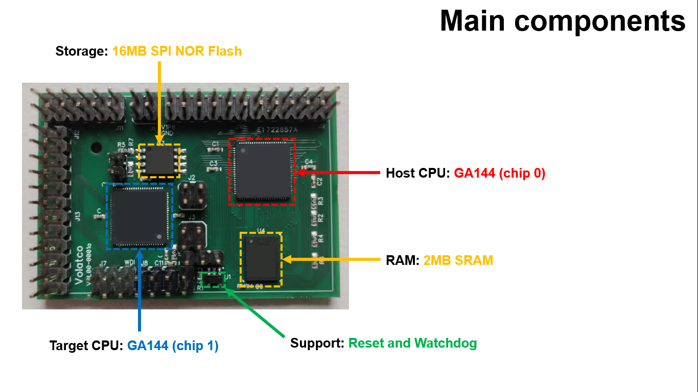
The platform includes two GA144A12 mesh-processor chips, 2 MB SRAM, 16 MB SPI flash, and exposed I/O via header pins.
Supported plug-in modules: Power and USB-connectivity, Ethernet, BLE, and external system interface.
polyForth: On-board lightweight dual-stack operating system and programming environment.
System summary
- 144 independent F18A computers.
- Up to 96B ops/s.
- ~13 uW idle to ~972 mW peak (~650 mW typical upper draw).
- One-gate start/stop latency (~100 ps).
- ~7 pJ per instruction.
- Event-driven compute: power used only when active.
Technical snapshot
- Architecture: ISLP GA144-based.
- Computers: 144 x 18-bit F18A processing nodes.
- Peak compute: up to 96 billion ops/s.
- Power per F18A: 90 nW idle leakage to 6.8 mW active.
- Power range per chip: 13 uW to 972 mW.
- Start and stop: one-gate delay (100 ps).
- Per-instruction energy: ~7 pJ.
The design supports deterministic low-latency behavior, with computers able to transition between active and inactive states in one gate delay.
Key Features
| Feature | Benefit |
|---|---|
| ISLP with dual GA144 (144 × 2 = 288 computers) | Run 288 concurrent threads that are ideal for parallel algorithms, machine-intelligence, and evolutionary computing. |
| polyForth® Runtime | A lightweight, stack‑based language that lets you prototype, debug, and iterate on AI kernels in minutes-no heavyweight SDKs required. |
| 2 MB SRAM + 16 MB SPI Flash | Fast volatile memory for model parameters and large non‑volatile storage for firmware, datasets, and compiled Forth programs. |
| Zero On‑Board Regulation | Power is supplied externally, eliminating regulator quiescent draw and shrinking the PCB. Choose the most efficient supply for your experiment. |
| Rich Off‑Board I/O | All GPIO, analogue‑in/out, and power pins are exposed on a standard breadboard‑compatible header. Plug in sensors, actuators, or custom expansion boards without soldering. |
| Watchdog & Reset Circuitry | Automatic recovery from software hangs, essential for long‑running experiments. |
| Modular Expansion Row | Connect external power modules, additional memory, Bluetooth, Ethernet, or bespoke I/O boards via header rows. |
| Compact Form Factor | Designed to fit into tight enclosures, drone payload bays, or multi‑board racks for scalable clusters. |
The information below pertains to the technical details of a Volatco.
The Volatco pin-set
All connections are made on the top of the PCB for Volatco model ‘a’. The model ‘b’ dialect has pins out both the top and bottom of the board.
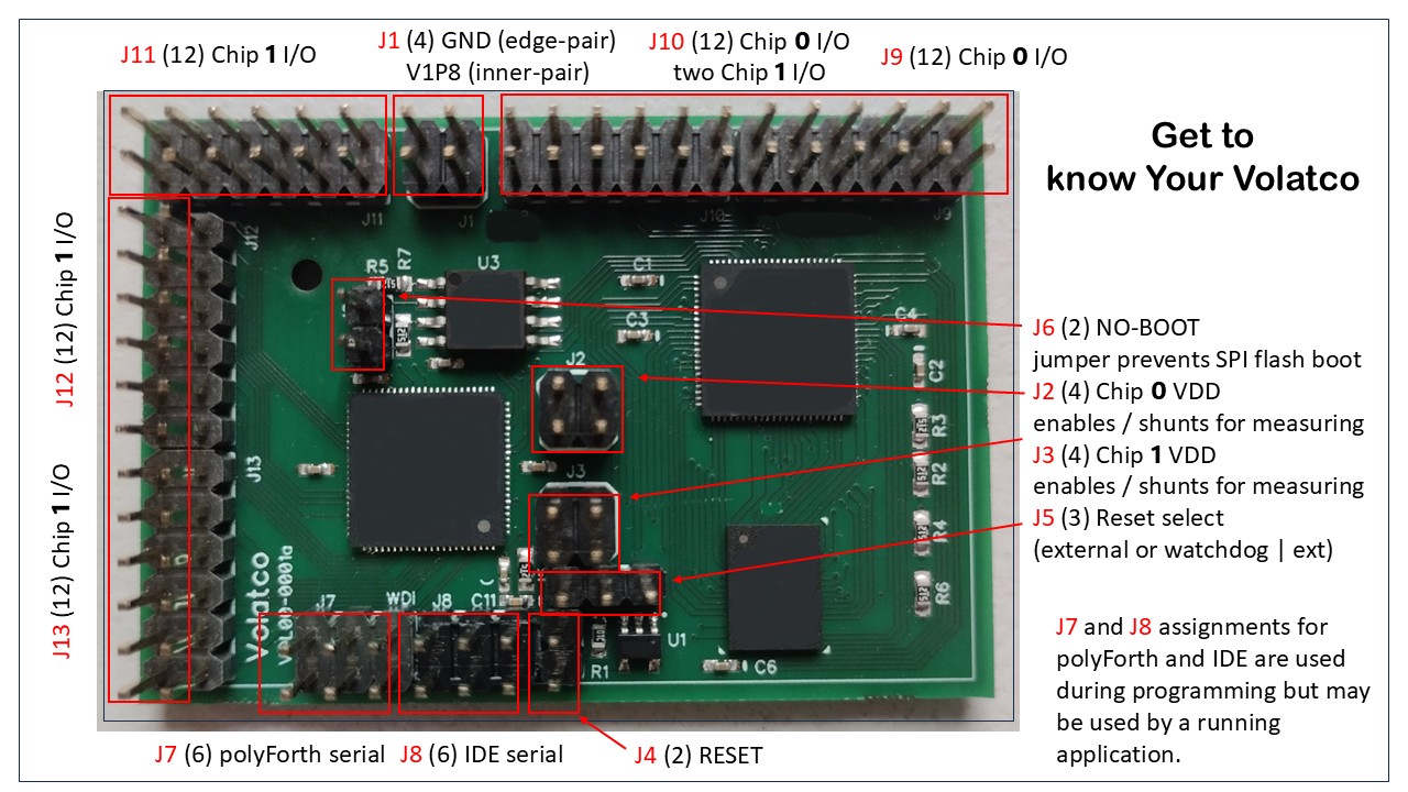
Option Jumpers
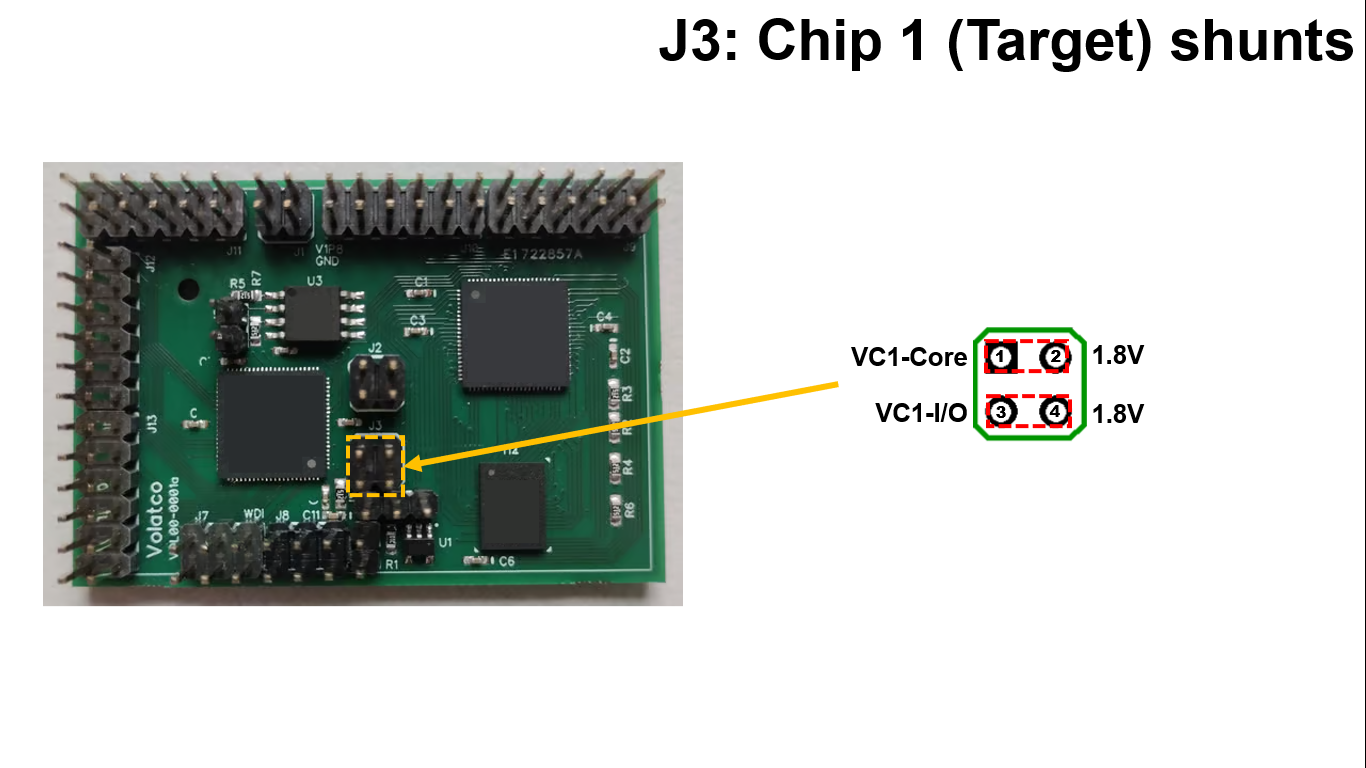
J6is “No boot”. Insert to preventchip 0from booting SPI flash on reset.J5selects development mode (pins 1 and 2 jumpered) or production (pins 2 and 3). In the latter case the watchdog/reset circuit is enabled. Development mode is required whenever “No boot” is installed.J4is shorted to produce a manual reset. This may also be done by the system providing IDE service throughJ8. Either of these reset methods works in either development or production mode.
Connection Headers
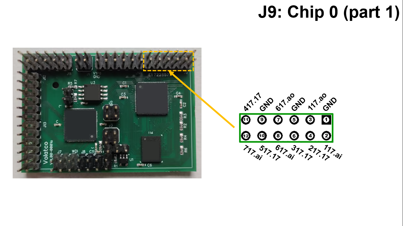
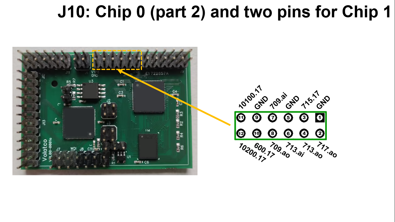
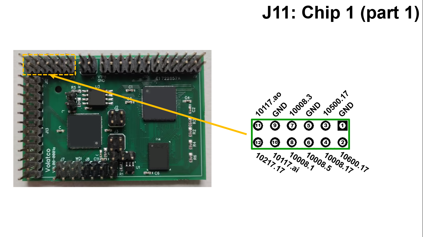
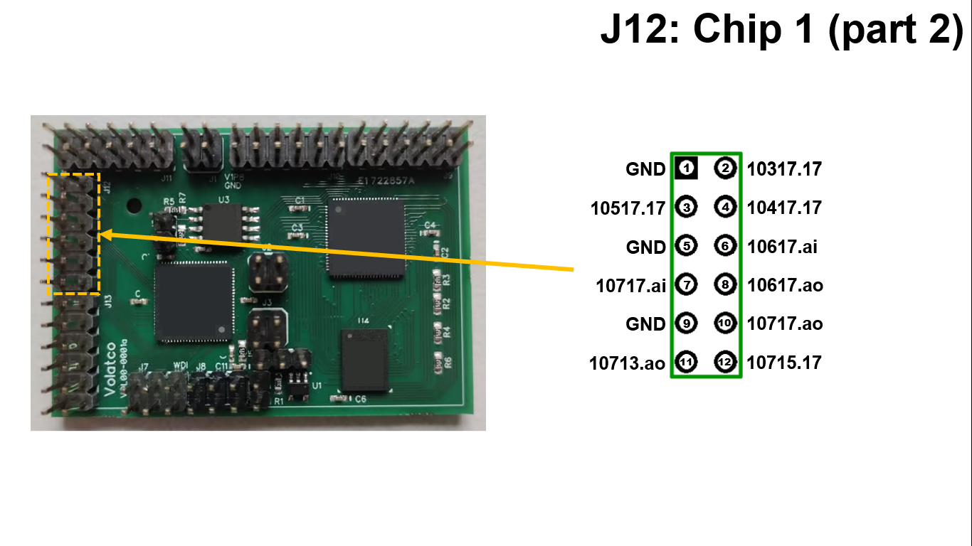
J1is external power and ground input.J8is for serial IDE input (including reset).J7is for polyFORTH terminal input - including watchdog signal, normally supplied from on the board. BothJ7andJ8carry both ground andV1P8for devices such as FTDI chips that can accept our supply to power their I/O pins.J9andJ10are signals from chip 0 plus two pins from chip 1.J11,J12, andJ13all carry signals fromchip 1. Each of these 12-pin headers carries 9 signals and 3 grounds, for a total of 45 signals. See following table for the pinout description.
Components
Power control
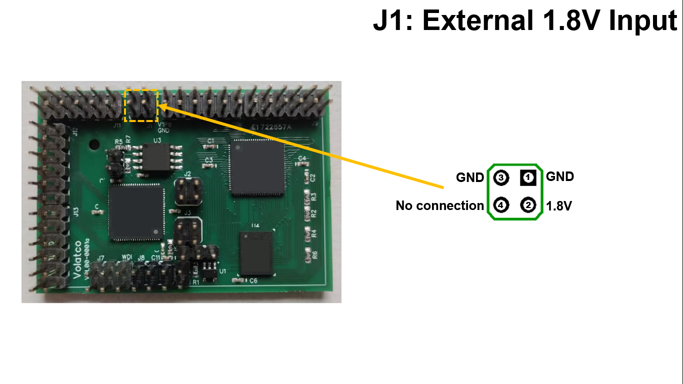
Note that the ground pins are those nearest the PCB edge. Also, pin 4 will depend on what is provided from the stacked module boards above or below.
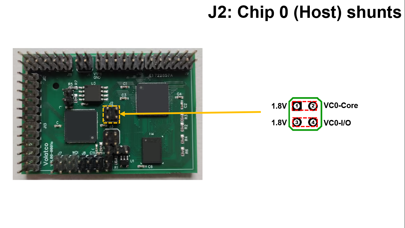
Jumpers are shown for normal operation. Substitute a shunt resistor to measure voltage drop across the resistor and calculate current. Be sure to use a small enough value that the expected current will not cause a voltage drop setting the supply below specs for the chip (typically 1.62V).
Note that unlike J2 the incoming supply is on the right side of this jumper block. The polarity of the drop will be reversed accordingly.
Manual reset
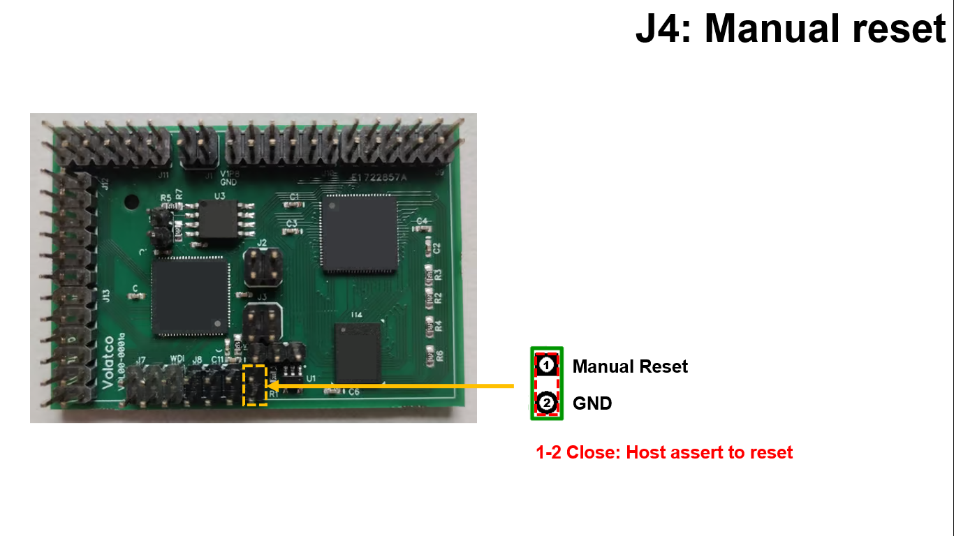
Short these pins together to assert reset on chip 0. Works in whether or not watchdog is enabled.
Operating modes
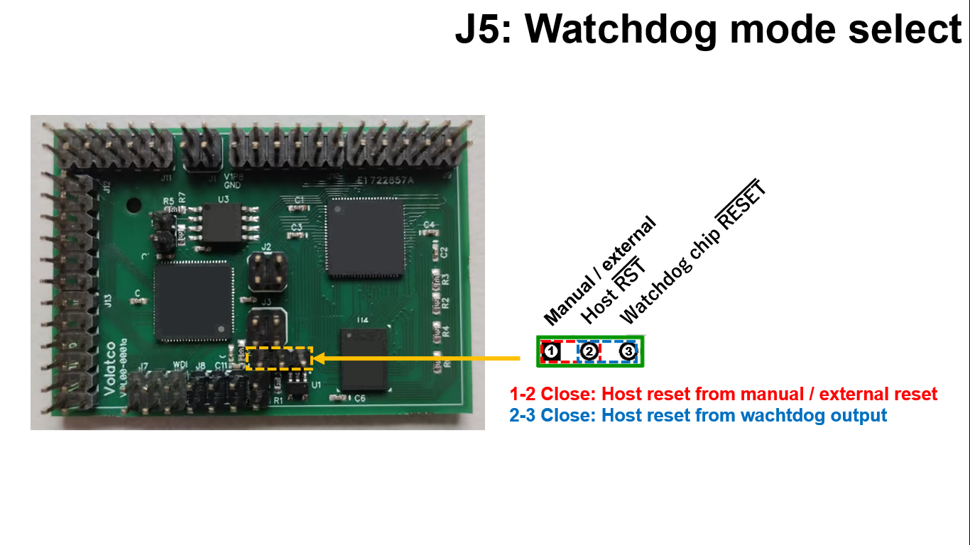
The manual/external reset always goes to the reset input of the watchdog chip. This jumper selects which signal goes to chip 0: The manual/external reset signal, or the output of the watchdog. Normal field production mode, enabling watchdog, is shown as the default. The watchdog should be disabled by moving the jumper to pins 1 and 2, when not running the production code on the chips.
No boot
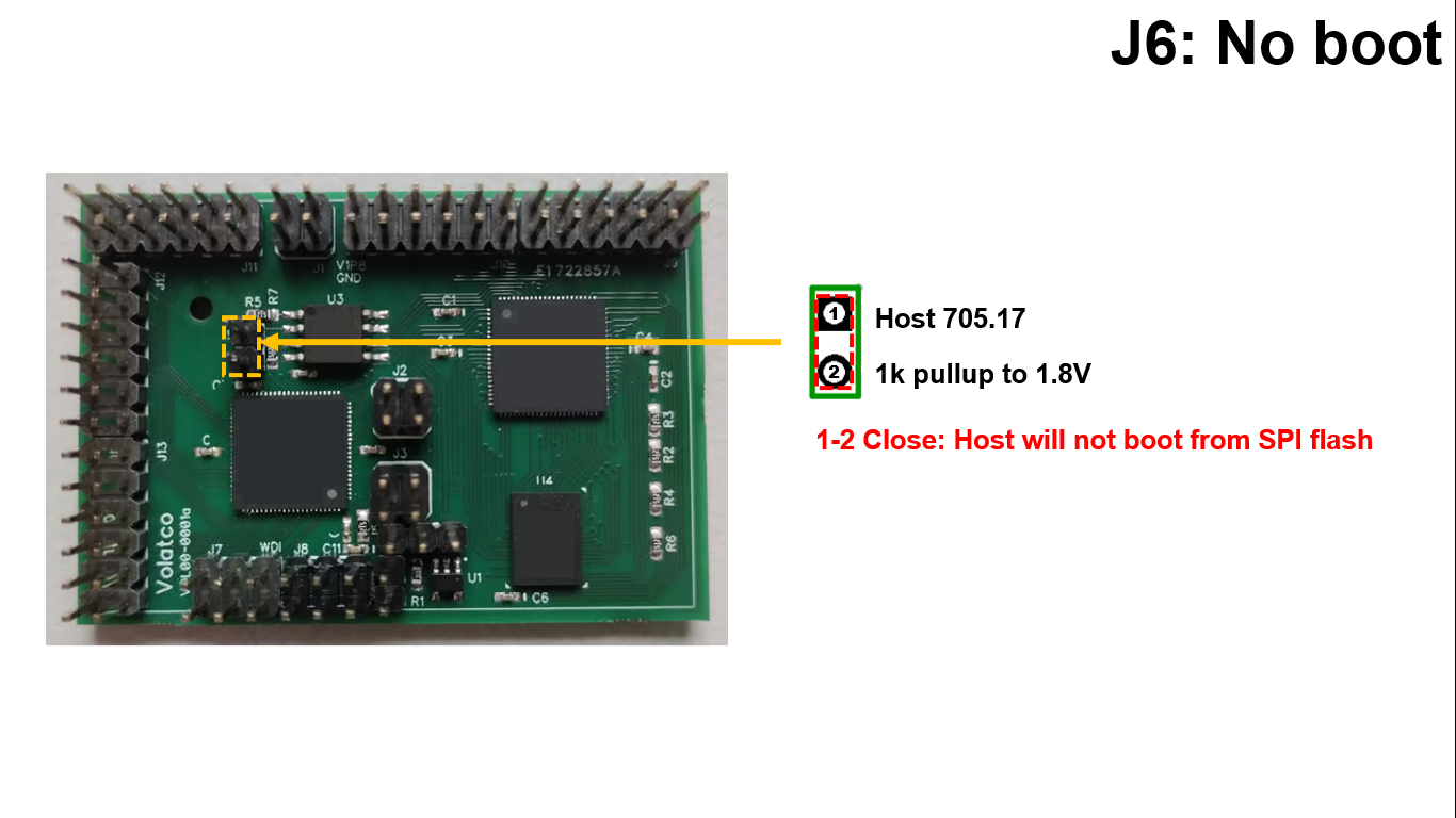
Install this jumper to prevent program booting from the SPI flash. When this is installed, the watchdog must be disabled by connecting pins 1 and 2 of J5.
Programmer access
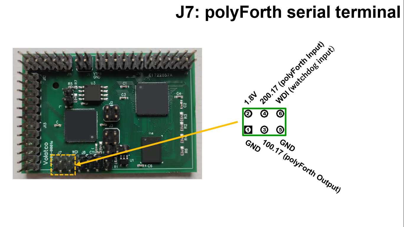
This serial port supports an asynchronous serial terminal for polyFORTH running on chip 0. Pin 6 must be jumpered or connected to a pin generating watchdog pulses before the watchdog may be enabled.
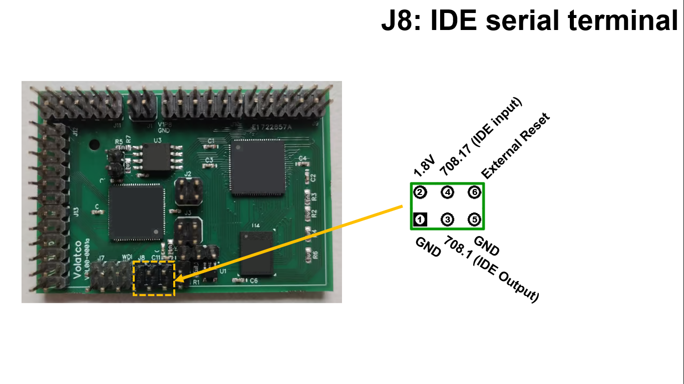
This serial port is used to talk to nodes on one or both chips directly using the Interactive Development Environment via node 708 of chip 0. Its reset pin is effective in both operating modes. Once the SPI flash has been initialized with boot code, this port is not necessary to run polyFORTH.
Signal access
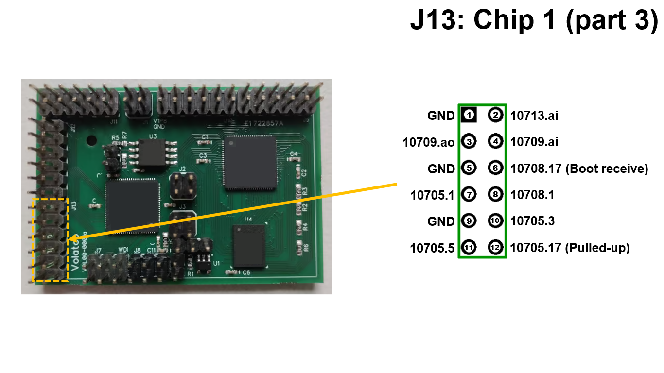
Be aware that pin 6 10708.17 is input to a boot node. If pin is being driven high by another device when chip 1 is reset, node 10708 will delay for a long time during boot which may cause problems with watchdog. If being used as an output and driven high on reset, the RC time constant of load capacitance and weak pull down resistance may be long enough to delay booting. The same is true of 10705.17 if being used as an input and driven low by another device during reset. Note that 10705.17 is pulled up with 5.1kΩ. If this pin is not being used it should be set to high impedance to minimize power consumption.
Forest Creature Adventures


The forest creatures are used as scenario guides for learning board behavior, power discipline, and asynchronous control patterns.

| Adventure | Objective | Hardware focus | Expected outcome | Artwork |
|---|---|---|---|---|
| Jezek and the Quiet Trail | Build a low-duty-cycle sensing loop that only wakes compute on events. | Wake/sleep transitions, watchdog-safe loops | Stable event logging with low idle draw. |  |
| Viver and the Signal Bridge | Forward sensor data between two nodes with bounded latency. | Inter-node messaging, pin routing | Repeatable packet transfer with measured timing. |  |
| Owl at J8 | Configure a robust serial debug session and reset workflow. | J8 IDE serial, manual reset via J4 |
Reliable flash/load/debug cycle during development. | 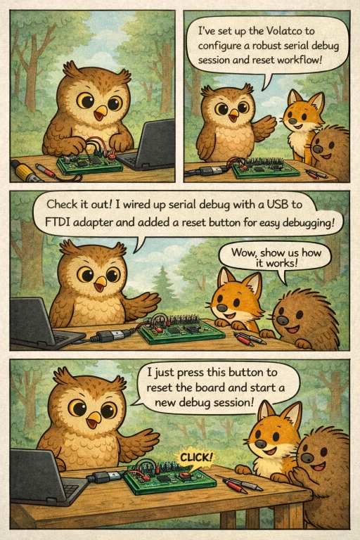 |
| Fox in the Rain | Validate graceful behavior under noisy or intermittent inputs. | Input filtering, timeout handling | No lockups during bursty/noisy signal tests. |  |
| Hedgehog Night Watch | Run long-duration watchdog validation with periodic health beacons. | J5 mode selection, watchdog pulse source on J7 |
Automatic recovery from forced hangs. |  |
| Badger Power Audit | Profile power across idle, active, and burst workloads. | Shunt measurement on J2/J3, workload scheduling |
Baseline power table for reproducible experiments. |  |
Suggested format for each adventure:
- Define the signal path and pin map.
- Define pass/fail criteria with measurable thresholds.
- Record power, latency, and recovery behavior.
- Save minimal reproducible polyForth program and test notes.
Related research
Agentic AI: Embodied Learning Model
Agentic AI is a foundational principle of the applicability of self-tuning controllers. Once the machine understand the ways and means of self-tuning constructs, it is an optimized model of the system under control, including analysis of damaged systems by close adaptation.
The ideal research path frames agency through embodied interaction rather than passive observation. In this view, an agent runs experiments, receives results, and updates behavior from those interactions.
The foundational module describes a cycle of anticipation, result comparison, and intrinsic states (for example frustrated, self-satisfied, and bored) that drive experiment switching and developmental learning over time.
Source pathway and branches: github.com/cartheur/ideal